Advanced Technology Adding a New Dimension to Metrology
25.10.2011 -
Microscopes have always been an indispensable tool for industry and technology. However, as a result of developments in digital photography and image editing, analysis and archiving, the application areas and possibilities for microscopes have changed radically over recent years. Modern materials manufacturing processes now require highly reliable and precise microscope system solutions for quality assurance purposes, such as observing surfaces, and also researching and analysing new materials and nanoparticles.
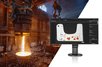
With its broad product spectrum, Olympus offers inspection and analysis solutions for all market areas, such as automotive, electronics, MEMS (Micro-Electro Mechanical System) and many more. It provides microscopes and accessories for routine tasks and high-end system solutions for inspection and metrology purposes, as well as devices for materials science research applications. Crucially, the company develops individual and innovative comprehensive solutions that integrate the microscope with advanced imaging software to create complete systems. One such advanced solution developed specifically for metrology applications is the LEXT – a new confocal laser scanning microscope for ultra-precise, highly reliable measurement and observation (Fig. 1).
Single Solution for Advanced Surface Analysis
Since it is exceptionally easy to use, LEXT makes inspections faster and more efficient. With outstanding 0.12 μm resolution and a magnification range from 120 x to 14,400 x, the new microscope is designed for researchers working between the limits of conventional optical microscopes and scanning electron microscopes (SEM). Combining UVmicroscopy and laser scanning confocal technology, LEXT enables high precision 3D surface profile observation and measurement in real time. Notably however, unlike SEM, any sample can be placed directly on the microscope stage without pre-treatment.
With much higher resolving power than conventional optical devices, but just as many different observation methods, every user can make quicker, more accurate specimen analysis with full traceability to international standards. LEXT is ideally suited for ultra-fine surface observation and measurements required for micro fabrication of devices like MEMS, for new materials development, and for today's thinner devices with more compact surface mounting requirements.
The exceptional resolution has been made possible by the sophisticated optical system specially designed by Olympus for operation at 408 nm (Fig. 2). This provides outstanding image resolution by minimising the aberrations associated with short wavelength illumination and maximising the 408 nm light source performance. Resolving power is further enhanced by confocal optics featuring an additional, optimised circular pinhole and a high speed XY scanner developed from Olympus MEMS technology. This results in the world-leading planar resolution which clearly resolves patterns of 0.12 μm line-width and profiles of 0.01 μm in height.
No Sample Preparation Required
In order for specimens to be studied using an electron microscope, they must fit into its chamber. This means that they are often fragmented and coated by vacuum-deposition which can take up to 20 minutes. The LEXT, however, allows observation and measurement without any of these time-consuming preparation steps.
Adding to its versatility, the maximum specimen load and height on the stage is 10 kg and 100 mm respectively. In addition, the standard manual stage can travel over a 100 mm2 area, enabling the precise location of the area of interest. Furthermore, since the observation method used is non-destructive, observation and measurement can be more efficiently performed whenever required.
Easy Application of Many Observation Methods
Similarly to optical microscopes, operating the new microscope requires no specialist knowledge – the image is visible as soon as the specimen is in place, enabling anyone to perform observation and measurement quickly and easily. Focusing on the specimen surface and finding the required position is achieved as rapidly and simply as a conventional microscope. Once the scan area has been defined by focusing on the top and bottom of the specimen surface, the scan process then runs automatically to produce outstanding images.
LEXT enables a wide variety of observation methods which are particularly valuable for multiphase analysis: -> 3D colour images for clear sample condition analysis
A unique feature is the ability to simultaneously image samples in 3D and 'true colour' by combining the laser image with the full colour brightfield image in the system computer. Defects in a colour filter or metal corrosion that can not be shown by monochrome observation are displayed by the system in clear 3D colour images, enabling much more comprehensive analysis than is possible by Scanning Electron Microscopy (SEM). -> Laser DIC function for more detailed surface observation
The laser DIC observation function makes it possible to observe minute surface indentations using 3D imaging. This exceptionally high degree of surface observation resolution is beyond the capabilities of conventional laser microscopes and matches that of SEM. -> Enhanced mode for imaging specimens with regions of differing reflection characteristic
Conventional laser microscopes cannot produce utilisable images of specimens which have a variety of reflective characteristics, such as the substrate surface and copper wiring surface of a printed circuit. LEXT offers an enhanced mode which enables such specimens to be clearly imaged. This same feature can also detect slanted samples which interfere with the laser reflection and are also problematic for conventional 3D measuring equipment.
Reliable, High-precision 3D Measurement
The new microscope's high repeatability applies not only to planar measurement, but also to every other aspect of 3D measurement and analysis, including depth, volume, surface area and roughness, which cannot be performed by an electron microscope (Fig. 3). Essential for height measurement, Z-axis scanning is precisely controlled by the use of a linear scale with 5 nm increments. In addition, the built-in Calculated Focus Operation (CFO) search function uses a sophisticated formula to calculate height information. Furthermore, there is absolutely no specimen contact during the measurement process, thereby eliminating any risk of damage.
To confirm the quality and reliability of data produced by LEXT, a strict traceability system is used. This conforms to international standards.
With its outstanding new observation and measurement capabilities, the LEXT is adding a new dimension to metrology. This enables more efficient processes for product manufacture, as well as a better understanding of surfaces and new findings to help engineers develop new materials with better properties.
Microscopes for All Reasons
The development of a new generation of microscope technology enabling the exceptional metrology capabilities of the LEXT has been made possible by Olympus’s heritage in the field of microscopy. A wide variety of microscopic capabilities are required within industry and technology and Olympus produces a broad range of upright, inverted and stereo microscopes and lighting equipment to meet these varying needs (Fig. 4). Combining microscope technology with sophisticated software for processing and analysing digital images, Olympus can deliver exceptionally innovative solutions and flexible products. These are designed to meet the evolving requirements of industry and technology for today and in the future – The new LEXT confocal laser scanning microscope is just one such shining example of many.
Contact: Esther Ahrent Section Manager Marketing Communication Olympus Life and Material Science Europa GmbH Microscopy Tel. +49-(0)40-23773 5426 microscopy@olympus-europa.com www.olympus-europa.com